In recent years, processors represented by CPUs and GPUs Driven by application needs, related design, manufacturing and packaging technologies are evolving. In terms of packaging, although the current 3D technology is very hot, for the vast majority of processors, 2D and 2.5D packaging technology is still mainstream, and the traditional MCM (Multi-Chip-Module, multi-chip module) has a second spring, and major CPU and GPU manufacturers are deploying products that use this packaging technology on a large scale.
An MCM is a module assembled on a substrate by two or more Die, or chip-sized package (CSP) ICs, forming an electronic system or subsystem, which can be a PCB, ceramic, or silicon wafer. The entire MCM can be packaged on a substrate or in the package. The MCM can be a standardized package for easy mounting on a circuit board, or an electronically capable module that can be mounted directly into an electronic system (PC, instrument, mechanical equipment, etc.).
MCM can be divided into the following three basic types:
MCM-L: MCM using a chip multilayer substrate, MCM-L is a high-density package PCB technology suitable for MCM using bonding and FC processes. MCM-L is not suitable for long-term reliability requirements and large use of environmental temperature differences.
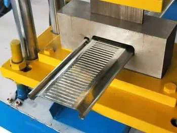
MCM-C: It is an MCM with a multilayer ceramic substrate, which is suitable for analog circuits, digital circuits, hybrid circuits, microwave devices and other applications. hmi panel
MCM-D: MCM using thin film technology, MCM-D substrate is composed of multiple layers of media, metal layers and substrates. The media layer is required to be thin, the metal interconnect should be small, and the appropriate interconnect impedance is available.
The advantages of MCM packaging can be summarized as the following three points: 1, can greatly improve the circuit connection density, improve the packaging efficiency; 2. Can complete the package design of “light, thin, short and small”; 3. It can improve the reliability of the package.
In recent years, SiP packaging technology has been deeply rooted in the hearts of the industry, so how does MCM compare with it? In fact, the development of chip packaging technology is a process of continuous progress and innovation, which is the collation, iteration, innovation and redevelopment of the original technology, and the same is true for MCM and SiP. MCM is packaged on a variety of high-density multilayer substrates, the main body is Die, and the circuits that make components are generally more complex, so MCM is an advanced hybrid integration technology. The market size and growth space of SIP is larger than that of MCM, and SIP is the product of the further development of MCM, which is the high-density assembly and interconnection of chips and components in different operating frequency bands. MCM mainly by stacking a variety of Die connection, few components, usually digital chips, memory-based, and SIP can encapsulate different process processes, different functions of chips, the chip can be accessed and exchanged between the signals, so as to achieve a system target product of all the interconnection, function and performance.
It can be seen that SiP is relatively advanced than MCM, but this does not affect the latter being adopted by more and more CPU and GPU vendors. Therefore, mature technology is not necessarily inferior to advanced technology, which is similar to the situation that mature process node technology is hot in recent years and production capacity is in short supply.
MCM CPUs are all the rage
For the CPU, MCM is not a new technology, as early as 1995, when Intel launched the Pentium Pro, it used MCM packaging technology to improve processor execution performance. In 2005, when the new Pentium D and Xeon 5000 series CPUs were released, they also used MCM packaging technology, which was the industry’s first dual-core CPU.
However, in the past decade, mainstream multi-core CPUs have adopted more native multi-core designs, until recent years, the number of cores of native multi-core design CPUs is difficult to have a higher growth, making MCM packaging technology re-emerge.
At present, more and more new generations of multi-core CPUs are beginning to use MCM packages. Around 2018, AMD adopted this technology when designing a 64-core server CPU. AMD’s design is ahead of Intel’s, at half the price of rival Xeon processors, and more power efficient. This was done because AMD adopted the strategy of “old design, new process”, “old design” is the mature MCM packaging technology, and “new process” is to use the most advanced 7nm process at that time to improve core density. In the past two years, AMD has further expanded this idea, which is the most popular Chiplet and its packaging technology.
For CPUs, especially server CPU manufacturers, multi-core products are already standard, because it not only consumes less power, but also improves yield a lot. Using MCM package design, manufacturers do not have to put all the cores into a single grain when designing a multi-core CPU, but can be designed into a multi-grain architecture, that is, a large core is split into multiple small cores, packaged in multiple grains, and then integrated into a single CPU. Compared with native multi-core designs, multi-core CPUs designed in MCM packages can achieve breakthrough growth and even double the number of cores, which is also one reason for the rapid growth of the AMD server CPU market in recent years.
Not only AMD, intel, which originally advocated native multi-core design, has also had to make compromises, and in recent years, when designing new multi-core CPUs, it has re-adopted MCM packaging to achieve more core count and higher performance.
After the release of the 10th generation OF HEDT high-end desktop processors in 2019, Intel has not launched a new HEDT product for more than two years, and the latest news shows that the company may launch Golden in the second half of 2022. Cove’s high-performance core HEDT products, primarily Sapphire? Rapids-AP。
In a recently leaked Xeon CPU benchmark, sources said that Intel is brewing sapphire? Rapids-AP new lineup, where “AP” was used in the flagship Cascade using the MCM package? Lake-AP product line. Sapphire? The Rapids-SP series has been designed with 4 MCM sets and each chip has up to 15 cores. Rapids-SP is considered a derivative of “AP”. It is reported that although the HEDT product line is aimed at the desktop market, Intel prefers to put it in the workstation market. As a product in an MCM package, Sapphire? The Rapids series includes many SKUs, and the thermal design power consumption of the flagship model can easily exceed 350W.
In recent years, Apple has been vying for the CPU market for Intel and AMD, especially notebooks Computers, Apple has achieved good results in a relatively short period of time. The CPU designed by the company also favors the MCM package design. In December 2021, some insiders showed the hidden part of the bottom of the M1 Max chip, as shown in the following figure, what is shown is MCM, and the main purpose of Apple’s use of this package design is to stack multiple Dies together, thereby greatly increasing the number of CPU and GPU cores.
GPU follows
With the increasing popularity of GPU applications in data centers, the MCM packaging technology originally used for CPUs has begun to penetrate into the GPU field, especially high-performance computing, which has received more and more attention in the industry.
Traditional graphics cards are PCB line cards with multiple GPUs that require a Crossfire or SLI bridge with two separate graphics cards connected. Traditional SLI and CrossFire require a PCIe bus to exchange data, textures, synchronization, and so on. Since rendering times between GPUs create synchronization problems, in many cases, traditional dual GPU graphics cards, i.e. two chips on a single PCB, are interconnected by it, each with its own VRAM. SLI or CrossFire consumes a lot of energy, and cooling is a challenge that has plagued engineers for a long time. The MCM is a separate package with an on-board bridge that replaces the traditional Crossfire or SLI bridge between two discrete graphics cards. In high-performance computing applications, this GPU in an MCM package has significant advantages.
The first to introduce MCM packaging technology to GPUs was AMD. In 2020, the company separated the GPU architecture of the game card from the professional card, the architecture of the game card is RDNA, and the architecture of the professional card is CDNA, and the first product is the Instinct MI100 series. In 2021, AMD’s Q2 earnings report confirmed that the CDNA 2 GPU has been shipped to customers, and its GPU core code name is Aldebaran, which became the company’s first product in an MCM package. On the PC side, after the introduction of the next-generation RDNA 3 architecture in 2022, MCM-based consumer Radeon GPUs will also emerge.
Manufacturing a multi-chip computing GPU is similar to making a multi-core MCM CPU, such as a Ryzen 5000 or Threadripper processor. First, bringing the chip closer together can improve computational efficiency. AMD’s Infinity architecture ensures high-performance interconnects, which are expected to make the efficiency of both chips close to one. Second, it is easier to mass-produce multiple small chips using advanced process techniques than large chips, because small chips are generally less defective and therefore have better yields than large chips.
Not long ago, AMD released a GPU based on the RDNA 3 architecture, that is, Radeon RX 7000, the latest graphics card in this series has three GPUs, namely Navi 31, Navi 32 and Navi 33, of which Navi 31 and Navi 32 will be in MCM package.
GPU giant Nvidia is also following up on MCM packaging.
Currently, NVIDIA’s scheme on MCM-encapsulated GPUs is called “Composable On Package GPU” (COPA). The COPA GPU architecture has the ability to mix/match multiple hardware blocks, making it better suited to today’s dynamic workloads and deep learning environments of high-performance computing. This consolidation is better suited to multiple types of workloads, resulting in higher levels of GPU multiplexing.

For the data center and consumer markets, NVIDIA has launched GPUs based on the Hopper architecture and the Ada Lovelace architecture, respectively. It is reported that the company will only use MCM technology on The Hopper architecture GPU, and the Ada Lovelace architecture GPU will still retain the traditional package design.
As Nvidia’s first GPU based on MCM technology, Hopper architecture products will use TSMC’s 5nm process process to support HBM2e and other connectivity features, competing with AMD’s CDNA 2 architecture products and Intel’s Xe-HP architecture GPUs.
In the research and development of independent graphics GPU, Intel lags behind a lot, seeing Nvidia in the GPU market, Intel can not sit still, in recent years in this area of vigorous investment, in order to catch up with the pace of the industry. In terms of MCM packaging GPUs, the company has also made new moves.
Not long ago, Intel announced a new patent describing how multiple compute modules work together to perform image rendering, indicating that the company’s GPU will be designed in an MCM package. In the new patent, Intel proposes a GPU image rendering solution that integrates multiple chips into the same unit to address issues such as manufacturing and power consumption while optimizing scalability and interconnectivity.
It is reported that Intel has integrated the checkerboard format rendering of the computing module, as well as distributed computing, so that the multi-chip design GPU has higher computing efficiency. Although the company did not go into the architectural details, it is estimated that intel Arc graphics cards equipped with MCM packaged GPUs are not far away.
In summary, whether it is CPU or GPU, major manufacturers are increasingly adopting MCM packaging technology, setting off a wave of “retro” boom.